1. Single segment without acceleration/deceleration pulse output PLSY
1. Single segment without acceleration/deceleration pulse output PLSY
1.1. nstruction Description
Single segment without acceleration/deceleration pulse output PLSY, the command can be used to output a specified number of pulses at a certain frequency. When a pulse is being output, the corresponding pulse output flag is set; When the number of output pulses reaches the set value, the pulse output stops and the corresponding pulse output flag is reset. During the pulse output process, the pulse and frequency are adjustable, and there is no acceleration or deceleration time when the frequency jumps.
When the input terminal is turned on, continuous output pulses start immediately at the set frequency. When the number of output pulses reaches the set number, the pulse output stops, and the number and frequency of process pulses can be adjusted. The 32-bit PLSY instruction can output a frequency range of 0Hz~200KHz.
For 16 point transistor type PLCs, Y0~Y1 are high-speed pulse output ports, and for 32/50/66 point transistor type PLCs, Y0~Y3 are high-speed pulse output ports; Relay type PLCs do not have high-speed pulse function, and the maximum output frequency of the output port is determined by the closing time of the relay. For multi pulse series PLCs, their high-speed pulse output ports are Y0~Y7 and Y10~Y11.
The instruction does not include a directional output port, and the directional signal output port number and signal control can be customized and set by the user.
| register | Pulse port |
|---|---|
| M8134 | Y000 |
| M8135 | Y001 |
| M8136 | Y002 |
| M8137 | Y003 |
| register | Pulse port |
|---|---|
| M8138 | Y004 |
| M8139 | Y005 |
| M8140 | Y006 |
| M8141 | Y007 |
| M8142 | Y010 |
| M8143 | Y011 |
| register | Pulse port |
|---|---|
| D8140(D8141) | Y000 |
| D8142(D8143) | Y001 |
| D8144(D8145) | Y002 |
| D8146(D8147) | Y003 |
| register | Pulse port |
|---|---|
| D8148(D8149) | Y004 |
| D8150(D8151) | Y005 |
| D8152(D8153) | Y006 |
| D8154(D8155) | Y007 |
| D8156(D8157) | Y010 |
| D8158(D8159) | Y011 |
1.1.1. Attention:
PLSY output frequency and output pulse number are 32-bit positive integers, occupying two consecutive D registers;
For high-speed pulse output, it is designed for external high-speed devices. To count the pulses, only the high-speed pulse input counter can be used, and internal counters cannot be used, nor can Y edge changes be used for counting;
The OFF time of transistors has the characteristic of being prolonged under light loads. So, when responsiveness is required, please design a load resistor to increase the load current when the load is lighter;
For the pulse output Y0, the number of pulses is accumulated in register D8140 (D8141), where D8141 stores the high 16 bits and D8140 stores the low 16 bits;
The pulse accumulation count registers (D8140~D8158) are important registers that can be read and written. When a new value is written, the count will be added or subtracted based on the new value;
Due to the fact that the pulse output of this instruction does not have a direction, the pulse accumulation count registers (D8140~D8158) can only count in the positive direction;
When outputting high-speed pulses, the values in the pulse accumulation count registers (D8140~D8158) are discontinuous and constantly changing. When used for judgment, please use size comparison instead of equal judgment.
When the pulse command is used to output port Y, the Y port cannot be used for other purposes, that is, ordinary commands cannot perform ON or OFF operations on the Y port anymore.
If the frequency of multiple pulse exceeds 200K, a pull-up resistor needs to be added to the pulse output port to ensure that the pulse waveform is not distorted. The pull-up voltage is 24V, and the recommended pull-up resistor is 1K.
1.2. The valid operands of the instruction
| Input/Output | Data Type | operand | Description |
|---|---|---|---|
| F | 32-bit integer | D/CV/K/H/FD, bit composite word (X/Y/M/C/T/S), local variable (LD) | frequency |
| P | 32-bit integer | D/CV/K/H/FD, bit composite word (X/Y/M/C/T/S), local variable (LD) | quantity |
| OUT | ON/OFF | Y | Pulse |
1.3. Example
Command table:
NETWORK 000
LDP M8151//M8151 rising edge assignment, must be rising edge to prevent PLC scanning from duplicate assignment
MOVD K400 D0//Initial frequency
NETWORK 001
LDP M1
MOVD K900 D0//Change the value D0
NETWORK 002
LDP M2
MOVD K650 D0//Change the value D0
NETWORK 003
LDP M3
MOVD K500 D0//Change the value D0
NETWORK 004
LD M0
PLSY D0 D2 Y000//When M0 is' 1 ', a pulse with a frequency of D0D1 is output at the Y000 port. When the number of pulses reaches D2D3, the output pulse stops and the pulse output flag M8134 is reset
Network 005
LDF M8134
RST M0 K1
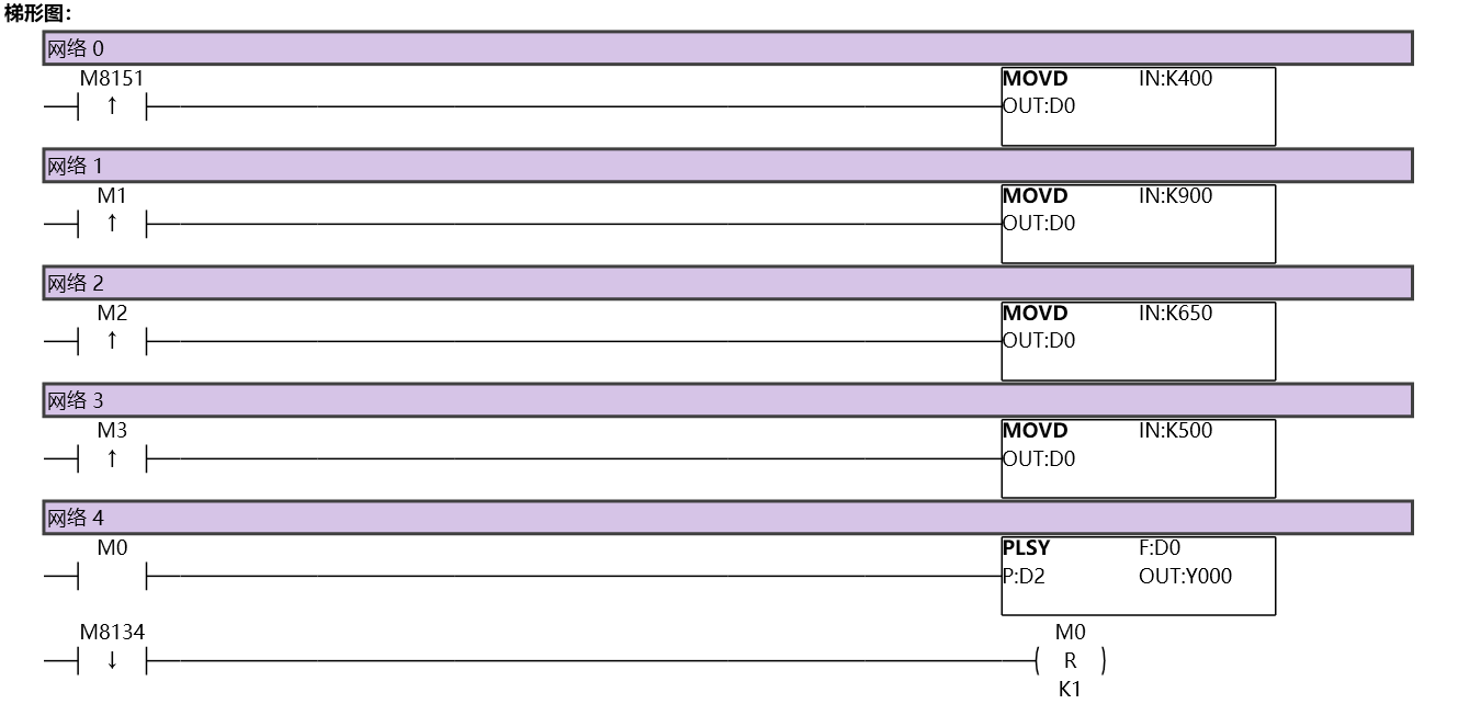
图1 PLSY11
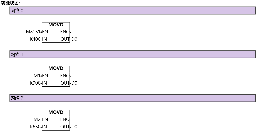
图2 PLSY12
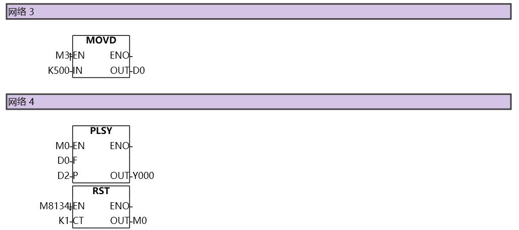
图3 PLSY13
1.3.1. Timing diagram:
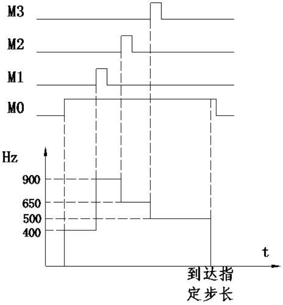
图4 Timing diagram