1. Single pulse output DRVI/DRVA
1. Single pulse output DRVI/DRVA
1.1. Instruction Description
Single segment pulse output DRVI/DRVA is a pulse output command with acceleration and deceleration that can be used to achieve a specified pulse frequency and number of pulses. When the input terminal is turned on, the pulse accelerates uniformly to the set frequency and outputs at a constant speed. When decelerating, it decelerates from the set frequency to 0, and the specified number of pulses is sent during the process. When the input terminal of the pulse command is disconnected, the pulse output immediately stops.
The DRVI/DRVA command can output frequencies ranging from 0Hz to 200KHz and pulse quantities ranging from K0 to K2147483647.
For 16 point transistor type PLCs, Y0~Y1 are high-speed pulse output ports, and for 32/50/66 point transistor type PLCs, Y0~Y3 are high-speed pulse output ports; Relay type PLCs do not have high-speed pulse function, and the maximum output frequency of the output port is determined by the closing time of the relay. For multi pulse series PLCs, their high-speed pulse output ports are Y0~Y7 and Y10~Y11.
The instruction can be used for asymmetric (acceleration and deceleration time set separately) single-stage trapezoidal and S-shaped position control. When the special function register M8069 is ON, the acceleration and deceleration of all pulse instructions are S-shaped, and when it is OFF, they are trapezoidal.
The special function register M8068 is used for directional polarity control. The default pulse direction output port is ON, which indicates the positive direction, and OFF, which indicates the negative direction. If M8068 is set to ON, the polarity of the directional output of all pulse commands will be reversed, with OFF indicating positive direction and ON indicating negative direction.
| register | pulse output |
|---|---|
| M8134 | Y000 |
| M8135 | Y001 |
| M8136 | Y002 |
| M8137 | Y003 |
| register | pulse output |
|---|---|
| M8138 | Y004 |
| M8139 | Y005 |
| M8140 | Y006 |
| M8141 | Y007 |
| M8142 | Y010 |
| M8143 | Y011 |
| register | pulse output |
|---|---|
| D8140(D8141) | Y000 |
| D8142(D8143) | Y001 |
| D8144(D8145) | Y002 |
| D8146(D8147) | Y003 |
| register | pulse output |
|---|---|
| D8148(D8149) | Y004 |
| D8150(D8151) | Y005 |
| D8152(D8153) | Y006 |
| D8154(D8155) | Y007 |
| D8156(D8157) | Y010 |
| D8158(D8159) | Y011 |
| register | pulse output |
|---|---|
| M8070 | Y000 |
| M8071 | Y001 |
| M8072 | Y002 |
| M8073 | Y003 |
| register | pulse output |
|---|---|
| M8074 | Y004 |
| M8075 | Y005 |
| M8076 | Y006 |
| M8077 | Y007 |
| M8078 | Y010 |
| M8079 | Y011 |
1.1.1. Attention:
For high-speed pulse output, it is designed for external high-speed devices. To count the pulses, only the high-speed pulse input counter can be used, and internal counters or Y edge changes cannot be used for counting. When used as a high-speed output, it cannot be used as a regular output port;
The OFF time of transistors has the characteristic of being prolonged under light loads. So, when responsiveness is required, please design a load resistor to increase the load current when the load is lighter;
For the pulse output Y0, the number of pulses is accumulated in register D8140 (D8141), where D8141 stores the high 16 bits and D8140 stores the low 16 bits;
The pulse accumulation count registers (D8140~D8158) are important registers that can be read and written. When a new value is written, the count will be added or subtracted based on the new value;
Due to the directional output of the pulse in this instruction, the pulse accumulation counting registers (D8140~D8158) count according to the direction;
When outputting high-speed pulses, the values in the pulse accumulation count registers (D8140~D8158) are discontinuous and constantly changing. When used for judgment, please use size comparison instead of equal judgment;
When the pulse command is used to output port Y, the Y port cannot be used for other purposes, that is, ordinary commands cannot perform ON or OFF operations on the Y port anymore;
If the frequency of multiple pulse exceeds 200K, a pull-up resistor needs to be added to the pulse output port to ensure that the pulse waveform is not distorted. The pull-up voltage is 24V, and the recommended pull-up resistor is 1K;
Be careful to avoid out of bounds situations, for example, if the current position is \ -100 and the DRVA command is sent to 2147483600, and the total length exceeds the upper limit of 32-bit positive integers, the target position will be incorrectly identified as \ -2147483594;
1.2. The valid operands of the instruction
| Input/Output | Data Type | operand | Description |
|---|---|---|---|
| F | 32-bit integer | D/CV/K/H/FD, bit composite word (X/Y/M/C/T/S), local variable (LD) | frequency |
| P | 32-bit integer | D/CV/K/H/FD, bit composite word (X/Y/M/C/T/S), local variable (LD) | quantity |
| AC | 16 bit unsigned integer | D/CV/TV/AI/AO/K/H/V/Z/FD, bit composite word (X/Y/M/C/T/S), local variable (LW) | acceleration time |
| DC | 16 bit unsigned integer | D/CV/TV/AI/AO/K/H/V/Z/FD, bit composite word (X/Y/M/C/T/S), local variable (LW) | deceleration time |
| OUT | ON/OFF | Y | Pulse |
| DIR | ON/OFF | Y | Direction |
1.3. Example
Command table:
NETWORK 000
LDP M8151
MOVD K100000 D0//Pulse output D0D1
MOVD K50000 D2//Pulse output frequency D2D3
MOV K100 D4//Acceleration time 100ms D4
MOV K200 D5//Deceleration time 200ms D5
NETWORK 001
LD M0
DRVI D0 D2 D4 D5 Y1 Y6//When M0 is set, DRVI starts working
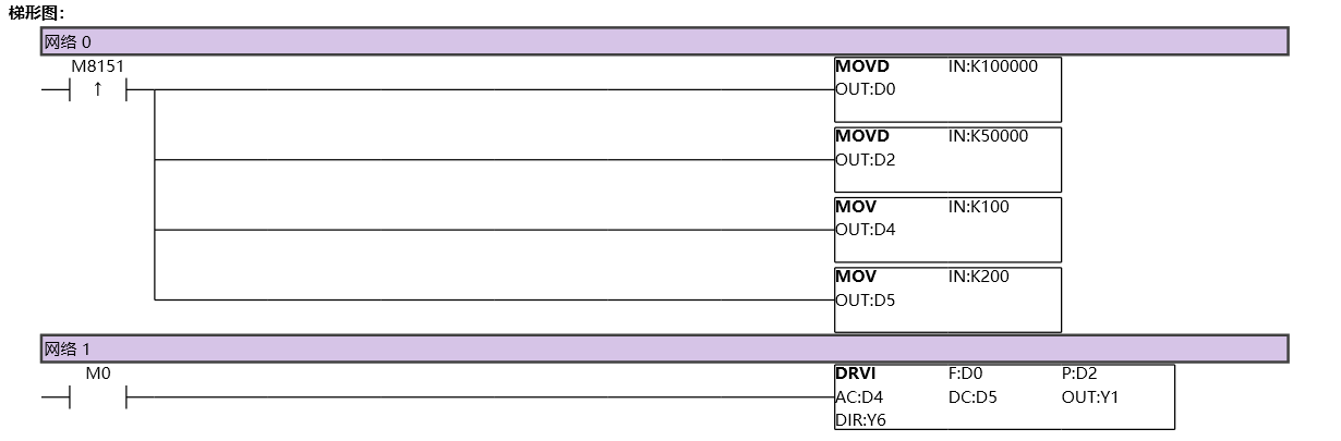
图1 DRVI11
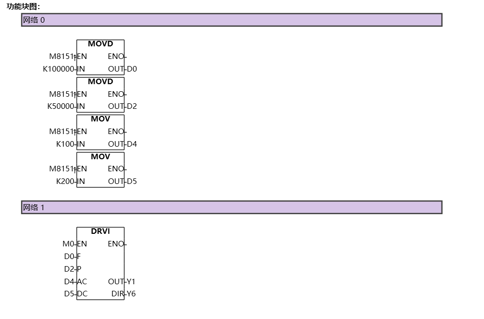
图2 DRVI12